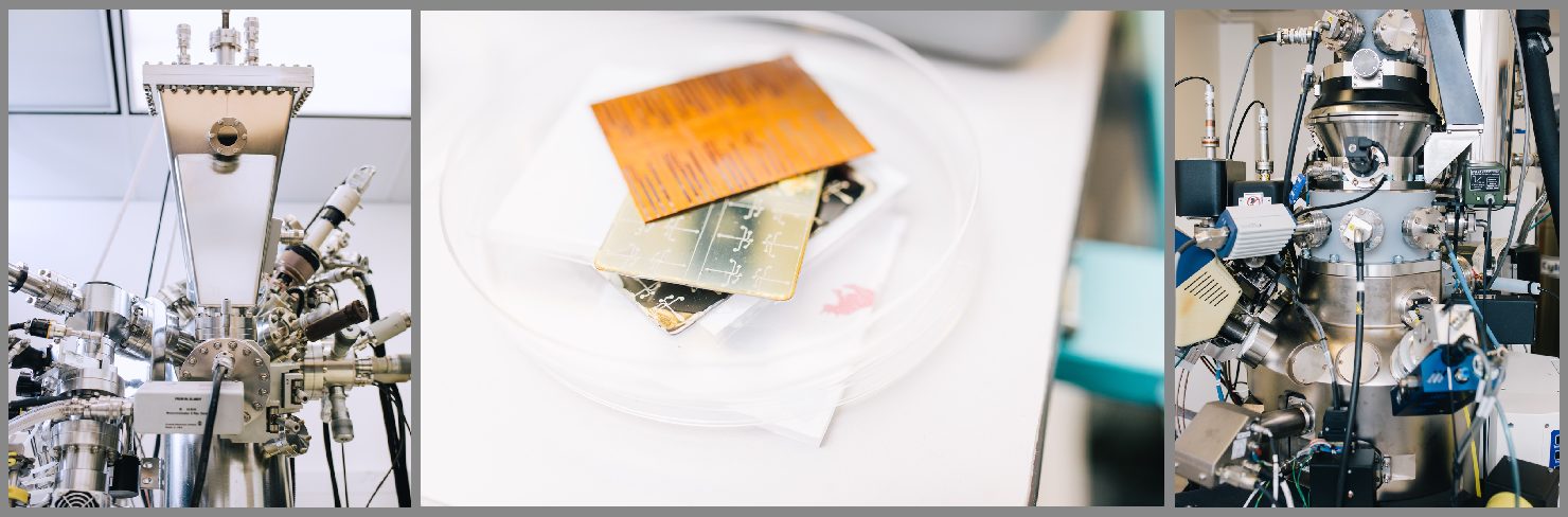
HIM
The HIM instrument is a Zeiss ORION NanoFab combining a specialized gas field-ionization source (GFIS) for the generation of He+ or Ne+ ions, with a conventional liquid-metal ion source (LMIS) for Ga+ ions. The ionization events of the imaging gas (He or Ne) at the GFIS are primarily localized to three atoms (the so-called trimer) that is formed at the pyramidal apex of a cryogenically-cooled tungsten tip held at a high positive potential. An aperture selects the ions generated from just one of the atoms of the trimer and the beam transported to the sample achieves a probe size of ~0.5 nm with a very low energy spread minimizing chromatic aberrations.
Imaging
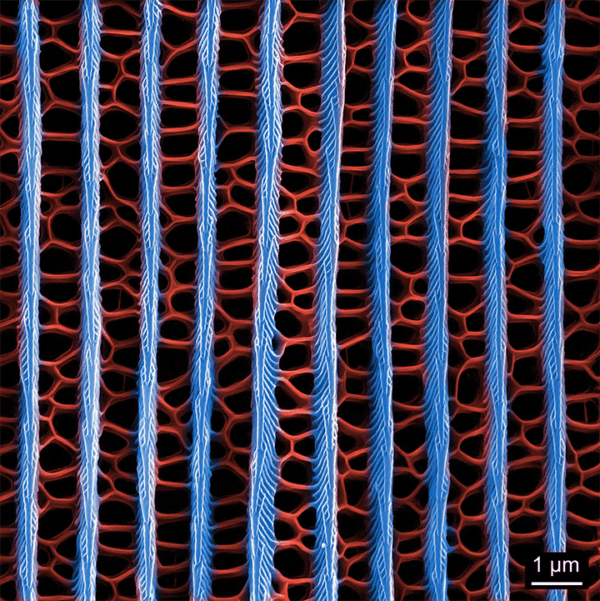
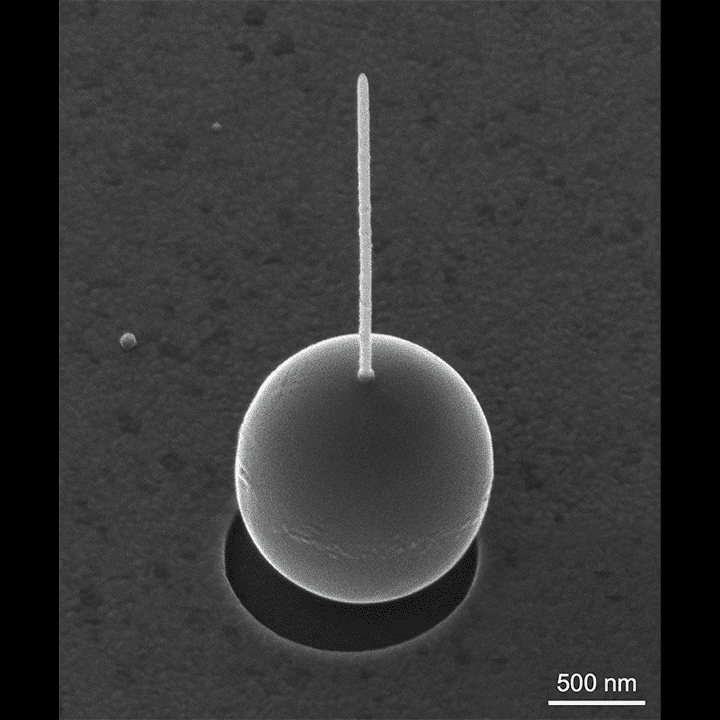
Imaging with all three beams is achieved by detecting the secondary electrons generated when the ions strike the sample, analogous to SEM. However, compared with the electron beam of the SEM, the interaction volume of the He+ beam with the specimen is very localized because there is much less scattering. In addition to high spatial resolution, HIM imaging is characterized by high surface sensitivity and a large depth-of-field. Charge-free imaging of insulating specimens is made possible using an electron flood gun.
Milling / Deposition / Implantation
For milling applications the multi-beam instrument also offers unique capabilities. The Ga+ beam can be used for bulk milling, after which features can be refined using the Ne+ beam and for the finest features the He+ beam is used. Complex patterns can be generated using the Nanopatterning and Visualization Engine. A gas injector system enables gas-assisted etching of silicon as well as ion-beam-induced deposition of tungsten and silicon dioxide. Nanoscale implantation studies using all three beams can also be performed.

")
Microscope Specifications
| He+ beam (GFIS) | 10 to 30 kV, 0.1 to 100 pA nominal probe size 0.5 nm |
| Ne+ beam (GFIS) | 10 to 30 kV, 0.1 to 10 pA nominal probe size 1.9 nm |
| Ga+ beam (LMIS) | 1 to 30 kV, 1 pA to 100 nA nominal probe size 2.9 nm |
| Detector | Everhart-Thornley SE detector |
| Gas Injector System | W, SiO2, XeF2 |
| Patterning Software | NPVE |
Publications
H. S. Choe, R. Prabhakar, G. Wehmeyer, F. I. Allen, W. Lee, L. Jin, Y. Li, P. Yang, C. Qiu, C. Dames, M. Scott, A. M. Minor, J.-H. Bahk, J. Wu, “Ion write micro-thermotics: programing thermal metamaterials at the microscale”, Nano Letters (2019), 19:6, 3830-3837, DOI: 10.1021/acs.nanolett.9b00984
H. S. Choe, J. Li, W. Zheng, J. Lee, J. Suh, F. I. Allen, H. Liu, H.-J. Choi, W. Walukiewicz, H. Zheng, J. Wu, “Anomalously high electronic thermal conductivity and Lorenz ratio in Bi2Te3 nanoribbons far from the bipolar condition”, Applied Physics Letters (2019), 114:15, 152101, DOI: 10.1063/1.5092221
R. C. Thayer, F. I. Allen, N. H. Patel, “Structural color in Junonia butterflies evolves by tuning scale lamina thickness”, bioRxiv preprint (2019), DOI: 10.1101/584532
F. I. Allen, N. R. Velez, R. C. Thayer, N. H. Patel, M. A. Jones, G. F. Meyers, A. M. Minor, “Gallium, neon and helium focused ion beam milling of thin films demonstrated for polymeric materials: study of implantation artifacts”, Nanoscale (2019), 11, 1403-1409, DOI: 10.1039/C8NR08224C
S. Saremi, R. Xu, F. I. Allen, J. Maher, J. C. Agar, R. Gao, P. Hosemann, L. W. Martin, “Local control of defects and switching properties in ferroelectric thin films”, Physical Review Materials (2018), 2:8, 084414, DOI: 10.1103/PhysRevMaterials.2.084414
Y. Yang, D. Frazer, M. Balooch, P. Hosemann, “Irradiation damage investigation of helium implanted polycrystalline copper”, Journal of Nuclear Materials (2018), 512, 137-143, DOI: 10.1016/j.jnucmat.2018.09.022
A. Mairov, D. Frazer, P. Hosemann, K. Sridharan, “Helium irradiation of Y2O3-Fe bilayer system”, Scripta Materialia (2018), 162, 156-160, DOI: 10.1016/j.scriptamat.2018.11.006
D. Simeone, M. Esposito, M. Scuderi, G. Calafiore, G. Palermo, A. De Luca, F. Todisco, D. Sanvitto, G. Nicotra, S. Cabrini, V. Tasco, A. Passaseo, M. Cuscunà, “Tailoring Electromagnetic Hot Spots toward Visible Frequencies in Ulta-Narrow Gap Al/Al2O3 Bowtie Nanoantennas”, ACS Photonics (2018), 5:8, 3399-3407, DOI: 10.1021/acsphotonics.8b00665
B. S. Archanjo, T. L. Vasconcelos, B. S. Oliveira, C. Song, F. I. Allen, C. A. Achete, P. Ercius, “Plasmon 3D Electron Tomography and Local Electric-Field Enhancement of Engineered Plasmonic Nanoantennas”, ACS Photonics (2018), 5:7, 2834-2842, DOI: 10.1021/acsphotonics.8b00125
S. M. Gilbert, S. Liu, G. Schumm, A. Zettl, “Nanopatterning Hexagonal Boron Nitride with Helium Ion Milling: Towards Atomically-Thin, Nanostructured Insulators”, MRS Advances (2018), 3:6-7, 327-331, DOI: 10.1557/adv.2018.117
G. Calafiore, A. Koshelev, T. P. Darlington, N. J. Borys, M. Melli, A. Polyakov, G. Cantarella, F. I. Allen, P. Lum, E. Wong, S. Sassolini, A. Weber-Bargioni, P. J. Schuck, S. Cabrini, K. Munechika, “Campanile Near-Field Probes Fabricated by Nanoimprint Lithography on the Facet of an Optical Fiber”, Scientific Reports (2017), 7, 1651, DOI: 10.1038/s41598-017-01871-5
Z. J. Wang, F. I. Allen, Z. W. Shan, P. Hosemann, “Mechanical behavior of copper containing a gas-bubble superlattice”, Acta Materialia (2016), 121, 78-84, DOI: 10.1016/j.actamat.2016.08.085
A. Koshelev, G. Calafiore, C. Piña-Hernandez, F. I. Allen, S. Dhuey, S. Sassolini, E. Wong, P. Lum, K. Munechika, S. Cabrini, “High refractive index Fresnel lens on a fiber fabricated by nanoimprint lithography for immersion applications”, Optics Letters (2016), 41:15, 3423-3426, DOI: 10.1364/OL.99.099999
G. Calafiore, A. Koshelev, F. I. Allen, S. Dhuey, S. Sassolini, E. Wong, P. Lum, K. Munechika, S. Cabrini, “Nanoimprint of a 3D structure on an optical fiber for light wavefront manipulation” (2016), 27:37, 375301, DOI: 10.1088/0957-4484/27/37/375301
T. C. Pekin, F. I. Allen, A. M. Minor, “Evaluation of neon focused ion beam milling for TEM sample preparation”, Journal of Microscopy (2016), 264:1, 59-63, DOI:10.1111/jmi.12416
J. Hong, A. Hadjikhani, M. Stone, F. I. Allen, V. Safonov, P. Liang, J. Bokor, S. Khizroev, “The Physics of Spin-transfer Torque Switching in Magnetic Tunneling Junctions in the Sub-10-nm Size Range”, IEEE Transactions on Magnetics (2016), 52:7, 1400504 DOI: 10.1109/TMAG.2016.2530622
Elsewhere on the Internet
Discover Magazine Media Gallery (slide 10) February 23 2018
Zeiss Microscopy News Blog June 27 2016
Zeiss Microscopy Instagram July 6 2016
Dr Ansgar Allen, University of Sheffield, UK, front-matter image
 The purchase of this instrument was made possible by an NSF grant from the Major Research Instrumentation program.
Contacts: Frances Allen and Paul Lum