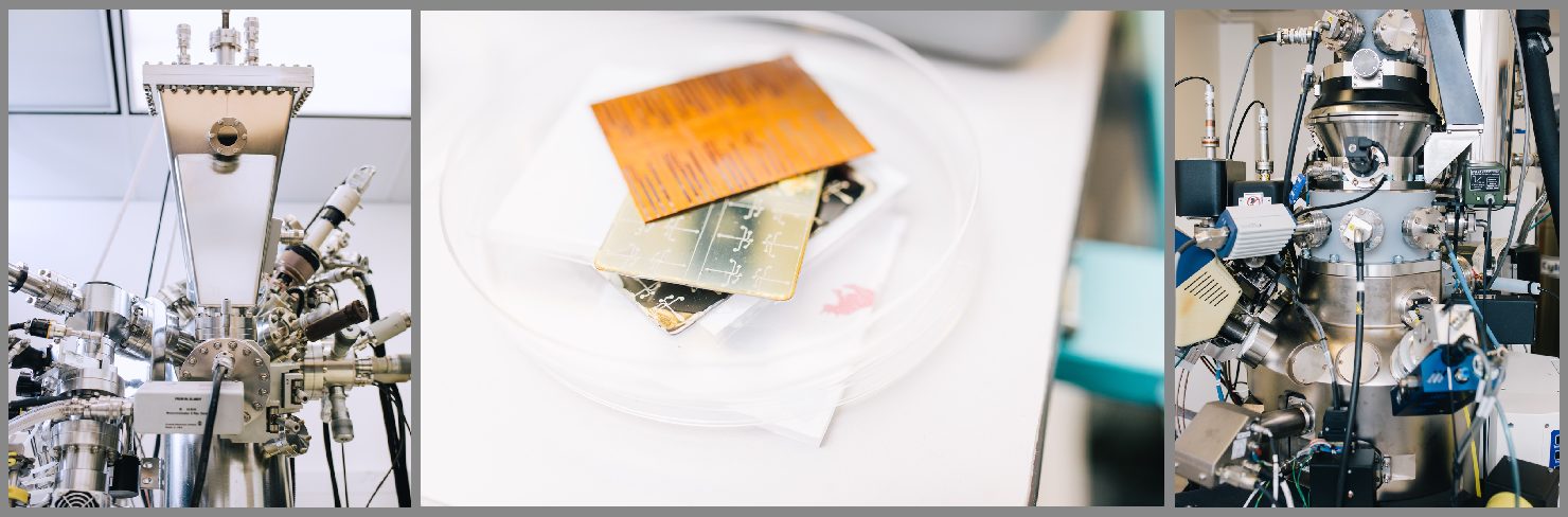
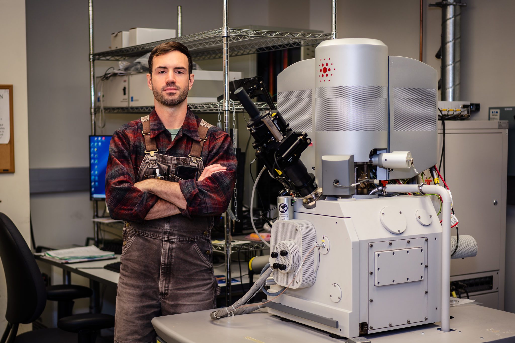
FIB-SEM
The FIB microscope is a dual-beam FEI Quanta machine, combining a Ga+ FIB column (liquid-metal ion source) and a field-emission SEM column in one tool. Through the addition of a variety of detectors, in-situ stage types and other accessories, this instrument enables a wide variety of sample preparation, manipulation and analysis to be performed in the same chamber. The microscope is also licensed to handle radioactive materials and plays a key role in the study of advanced materials for nuclear applications.
Milling/Etching
The Ga+ beam is used for site-specific etching of materials for the fabrication of electron-transparent specimens for transmission electron microscopy (TEM), sharp tips for atom-probe tomography (APT), pillar samples for in-situ mechanical testing, and further structures of interest for micro- and nanofabrication applications.
Microanalysis
Materials analysis is made possible using the electron beam for high-resolution Z-contrast imaging in combination with an electron backscatter detector for crystallographic orientation mapping by electron backscatter electron diffraction (EBSD), and an x-ray detector for elemental mapping by x-ray energy-dispersive spectrometry (XEDS). The Ga+ beam can also be used for fine texture analysis in crystalline materials. Recently, a detector for scanning transmission electron microscopy (STEM) has also been installed.
Deposition
Ion- and electron-beam-assisted deposition of platinum can be used to form nanoscale electrical contacts for rapid prototyping and analysis of novel electronic structures and materials, and for the deposition of a protective layer prior to ion-beam etching for cross-sectional analysis.
In-situ Capabilities
Micromanipulators within the chamber can be used for electrical probing or for positioning of samples with nanoscale precision (e.g. for TEM lift-outs). A micro-indenter and pico-indenter are available for in-situ mechanical testing, and a cold stage enables materials analysis down to cryo-level temperatures. A cryo-transfer stage enables the transfer of frozen specimens into the chamber for micromachining and imaging, and subsequent transfer back out of the microscope for high-resolution analysis by cryo TEM.
Microscope Specifications (including various detectors and other add-ons)
| Ga+ beam | 2 to 30 kV; 1.5 to 65 nA nominal resolution 7 nm at 30kV |
| Electron beam | 0.5 to 30kV; 4 to 48nA nominal resolution 1.2 nm at 30kV |
| Deposition materials | Pt |
| Detectors available | SE (secondary electron), XEDS, EBSD, STEM |
| In-situ stages and accessories | Micro-manipulators (Kleindiek) Pico-indenter (Hysitron PI 85) Cryo-stage (Hummingbird) Cryo-transfer stage (Hummingbird) |
Contacts: Paul Lum and Frances Allen
Recent Publications
Frazer, D., M. D. Abad, D. Krumwiede, C. A. Back, H. E. Khalifa, C. P. Deck, and P. Hosemann. “Localized mechanical property assessment of SiC/SiC composite materials.”Composites Part A: Applied Science and Manufacturing 70 (2015): 93-101.
Lupinacci, A., J. Kacher, A. Eilenberg, A. A. Shapiro, P. Hosemann, and A. M. Minor. “Cryogenic in situ microcompression testing of Sn.” Acta Materialia 78 (2014): 56-64.